メインコンテンツに移動
以下のデバイスを代替品として推奨しております。
5P83905 - 1.8V to 3.3V 1:6 Crystal Input to LVCMOS Output High-Performance Clock Fanout Buffer with OE
Functional replacement5PB1106 - 1.8V to 3.3V 1:6 LVCMOS High-Performance Clock Buffer
Functional replacement for 83905AMLF

概要

説明

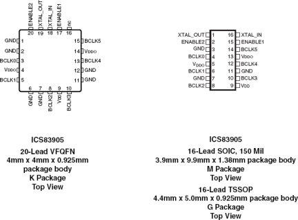
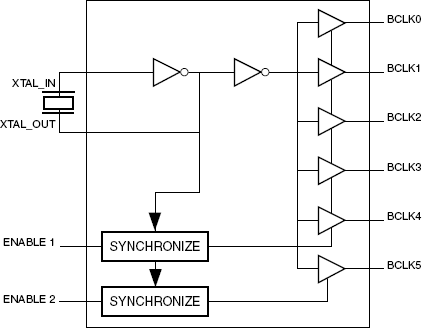
The 83905 is a low skew, 1-to-6 LVCMOS / LVTTL Fanout Buffer. The low impedance LVCMOS/LVTTL outputs are designed to drive 50Ω series or parallel terminated transmission lines. The effective fanout can be increased from 6 to 12 by utilizing the ability of the outputs to drive two series terminated lines. The 83905 is characterized at full 3.3V, 2.5V, and 1.8V, mixed 3.3V/2.5V, 3.3V/1.8V and 2.5V/1.8V output operating supply mode. Guaranteed output and part-to-part skew characteristics along with the 1.8V output capabilities makes the 83905 ideal for high performance, single ended applications that also require a limited output voltage.

特長

  • Six LVCMOS / LVTTL outputs
  • Outputs able to drive 12 series terminated lines
  • Crystal Oscillator Interface
  • Crystal input frequency range: 10MHz to 40MHz
  • Output skew: 80ps (maximum)
  • RMS phase jitter @ 25MHz, (100Hz – 1MHz): 0.26ps (typical), VDD = VDDO = 2.5V
    Offset                  Noise Power
    100Hz.................-129.7 dBc/Hz
    1kHz...................-144.4 dBc/Hz
    10kHz.................-147.3 dBc/Hz
    100kHz...............-157.3 dBc/Hz
  • 5V tolerant enable inputs
  • Synchronous output enables
  • Operating power supply modes:
    Full 3.3V, 2.5V, 1.8V
    Mixed 3.3V core/2.5V output operating supply
    Mixed 3.3V core/1.8V output operating supply
    Mixed 2.5V core/1.8V output operating supply
  • 0°C to 70°C ambient operating temperature
  • Available in lead-free (RoHS 6) package

製品比較

アプリケーション

ドキュメント

設計・開発

モデル

ECADモデル

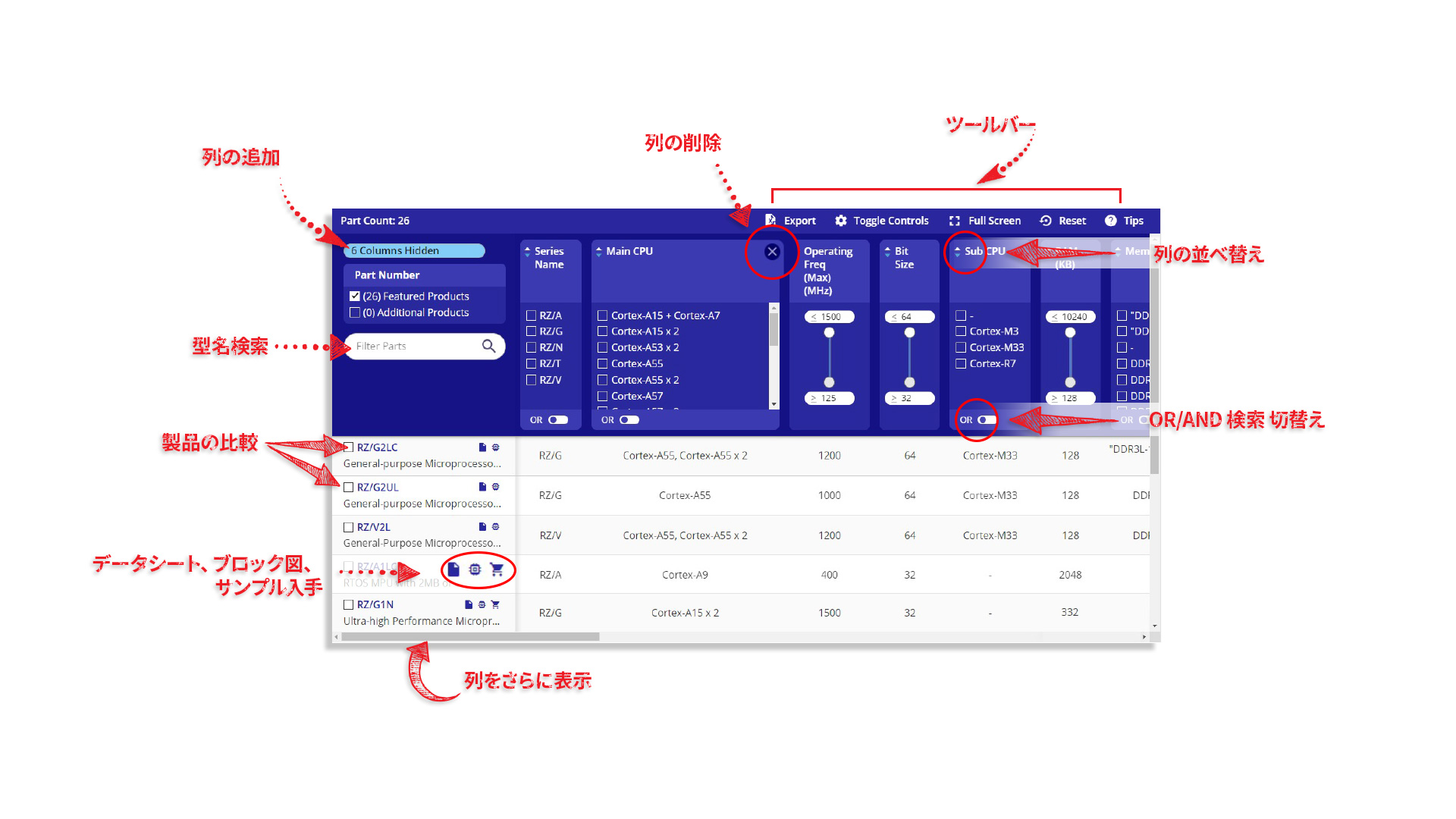
[製品選択]テーブル内の製品名をクリックするとSamacSysが提供する回路図シンボル、PCBフットプリント、3D CADモデルがご確認いただけます。 お探しのシンボルやモデルが見つからない場合、Webサイトから直接リクエストできます。

Diagram of ECAD Models

ビデオ&トレーニング

Fanout Buffers Overview by IDT

Description

Provides an overview of the features and benefits of IDT's industry-leading fanout buffer and clock distribution portfolio. Fanout buffers are a useful building block of many clock trees, providing signal buffering and multiple low-skew copies of the input signal. The clock fanout from a single input reduces loading on the preceding driver and provides an efficient clock distribution network. Presented by Vik Chaudhry, technical marketing manager at IDT. For more information about Renesas's clock IC timing solutions, visit the Clock Buffers & Drivers page.


Transcript
Thank you for joining us for an overview of IDT's Fanout Buffers. My name is Vik Chaudhry. I'm Marketing Manager for IDT's timing products.
 
Here's the agenda for this presentation. We'll start with a brief introduction of buffers and clock distribution devices, then I'll show you some examples of differential and single-ended buffers. We'll discuss zero delay buffers, and then some examples of how these devices are used in actual circuits. 
 
Buffers are one of the most important building blocks of a clock tree. Typically, they have one or two inputs, and multiple outputs. IDT has a very large portfolio of buffers. That includes Non-PLL buffers, PLL-based delay zero buffers, buffers with multiplexes, and dividers. IDT has about 450 such devices that supports various versions of inputs and output styles. In many cases, buffers can also be used as level translators to convert one signal level to another. IDT buffers are designed for low-additive phase jitter and low skew in mind. Many of them have differential architecture internally for better use of common mode projection ratio.
 
The first set of buffers are ones with differential outputs. Differential signals are becoming very popular these days with high speed applications. Various differential levels, such as LVDS, LVPECL, HCSL are supported by IDT buffers. We offer parts that have up to 24 different outputs and which go up to 3GHz in speed. These parts are available in both industrial as well as commercial temperature ranges. As I mentioned earlier, these parts are designed for very low additive phase noise in mind. You will find that additive phase noise is listed in the EC tables at the back of the data sheets, and in many cases, you can also see a phase noise plot in the back of the data sheets, too. Here is an example of 853S006 device which has one input and six outputs. And in this slide you also see the additive phase noise for this device.
 
Here are some more examples of differential buffers. One important thing to note is that in these cases, one, the input level is single-ended, so the device acts as a level translator. Second, that these devices have marks built into them.  In one case we have two single-ended signals coming in. In the other case we have LVCMOS input and a crystal input. Also worth noting is that all output signals are synchronized with the enabled signal, so they are all phase aligned. 
 
854105 is another example of a simple, one to four buffer which has individual output enabled pins. 879S216, as you can see on the bottom of the screen, has a MUX, divider, and fanout buffer, all combined into one flexible device. Such devices can not only provide the fanout, but in some cases, they can build the whole clock tree for a customer. 
 
Now, let's consider some single-ended buffers. In this example we have a differential signal, or a crystal input coming in that is fanned out to ten single-ended LVCMOS signals. Typically, the differential inputs can accept either LVDS, LVPECL, and HCSL or HSTL levels. 
 
This is an example of a very flexible device, where one, we have a MUX at the input stage, two we have two sets of dividers that are independent of each other, and three, there are two sets of fanout buffers for each of the banks that enable signal for each bank. So as you can see, there are various flavors of fanout buffers available in IDT's portfolio. 
 
We also have zero delay buffers in our portfolio. A zero delay buffer is a PLL-based device that provides an output that is in phase alignment with the input signal. In this category of devices, we have parts with multiple outputs, different levels of inputs and outputs, and different divider ratios. Designers like these types of devices when they want really tight control over timing of their board. 
 
This slide shows different applications of the fanout buffer. Typically, we see clocks fanout to different phys, processors and cores, on a typical board. In some applications designers want these clocks to be synchronized for timing. In the second case a zero delay buffer is used to divide the clock and then distribute it over the board. 
 
Buffers can sometimes help designers reduce the cost and the total BoM of their boards also. In this example, the original board used eight different crystals to clock the different phys switches, and fabric. With the use of 8538-26, we were able to replace all of the crystals with basically two parts, a crystal, and a fanout buffer. It helped to reduce the overall cost of the board, and it also reduced the lead times for the crystals that were used on this board. 
 
As I mentioned earlier, IDT has a very large portfolio of fanout and clock distribution devices. To make it easy to select these parts we have developed collateral that can be used. This collateral is located on the IDT website under clock and timing products. If you look under fanout buffers and dividers, you will see this collateral available. This is a very handy tool to expedite selection of parts.
 
We also have excellent application support for all the clocks and clock distribution devices. Most of our products include IBIS models. We also have application notes for various termination schemes, filter recommendations, and we also review schematics. If you have any questions, please feel free to either drop us an email at [email protected] or [email protected]
 
Thank you for choosing IDT timing products.