概要
説明
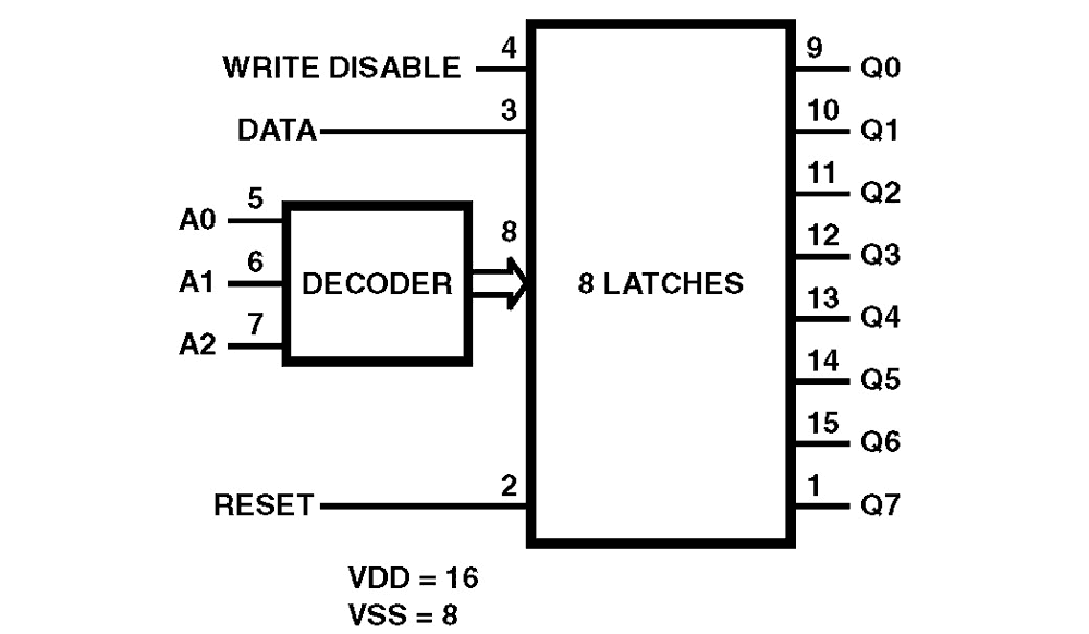
The CD4099BMS 8-bit addressable latch is a serial input, parallel output storage register that can perform a variety of functions. Data are inputted to a particular bit in the latch when that bit is addressed (by means of inputs A0, A1, A2) and when WRITE DISABLE is at a low level. When WRITE DISABLE is high, data entry is inhibited; however, all 8 outputs can be continuously read independent of WRITE DISABLE and address inputs. A master RESET input is available, which resets all bits to a logic 0 level when RESET and WRITE DISABLE are at a high level. When RESET is at a high level, and WRITE DISABLE is at a low level, the latch acts as a 1 of 8 demultiplexer; the bit that is addressed has an active output that follows the data input, while all unaddressed bits are held to a logic 0 level. The CD4099BMS is supplied in these 16-lead outline packages: Braze Seal DIP H4X, Frit Seal DIP H1F, Ceramic Flatpack H6W.
特長
- High-voltage type (20V rating)
- Serial data input
- Active parallel output
- Storage register capability
- Master clear
- Can function as demultiplexer
- 100% tested for quiescent current at 20V
- 5V, 10V and 15V parametric ratings
- Standardized symmetrical output characteristics
- Maximum input current of 1µA at 18V over full package temperature range; 100nA at 18V and +25 °C
- Noise margin (over full package temperature range) 1V at VDD = 5V, 2V at VDD = 10V, 2.5V at VDD = 15V
- Meets All Requirements of JEDEC tentative standard No. 13B, "Standard Specifications for Description of 'B' Series CMOS Devices"
製品比較
アプリケーション
- Multi-line decoders
- A/D converters
設計・開発
モデル
ECADモデル
[製品選択]テーブル内の製品名をクリックするとSamacSysが提供する回路図シンボル、PCBフットプリント、3D CADモデルがご確認いただけます。 お探しのシンボルやモデルが見つからない場合、Webサイトから直接リクエストできます。

Processing table
| SBDIP | 16 | Tube | Not Applicable | 2.5 | 20.3 x 7.5 x 2.41 | 5962R9661501VEC | Yes | Gold Plate over compliant Undercoat-e4 | 25 | -55 to +125°C | ||
| CFP | 16 | Tray | Not Applicable | 1.3 | 10.4 x 6.9 x 0.00 | 5962R9661501VXC | Yes | Gold Plate over compliant Undercoat-e4 | 25 | -55 to +125°C |
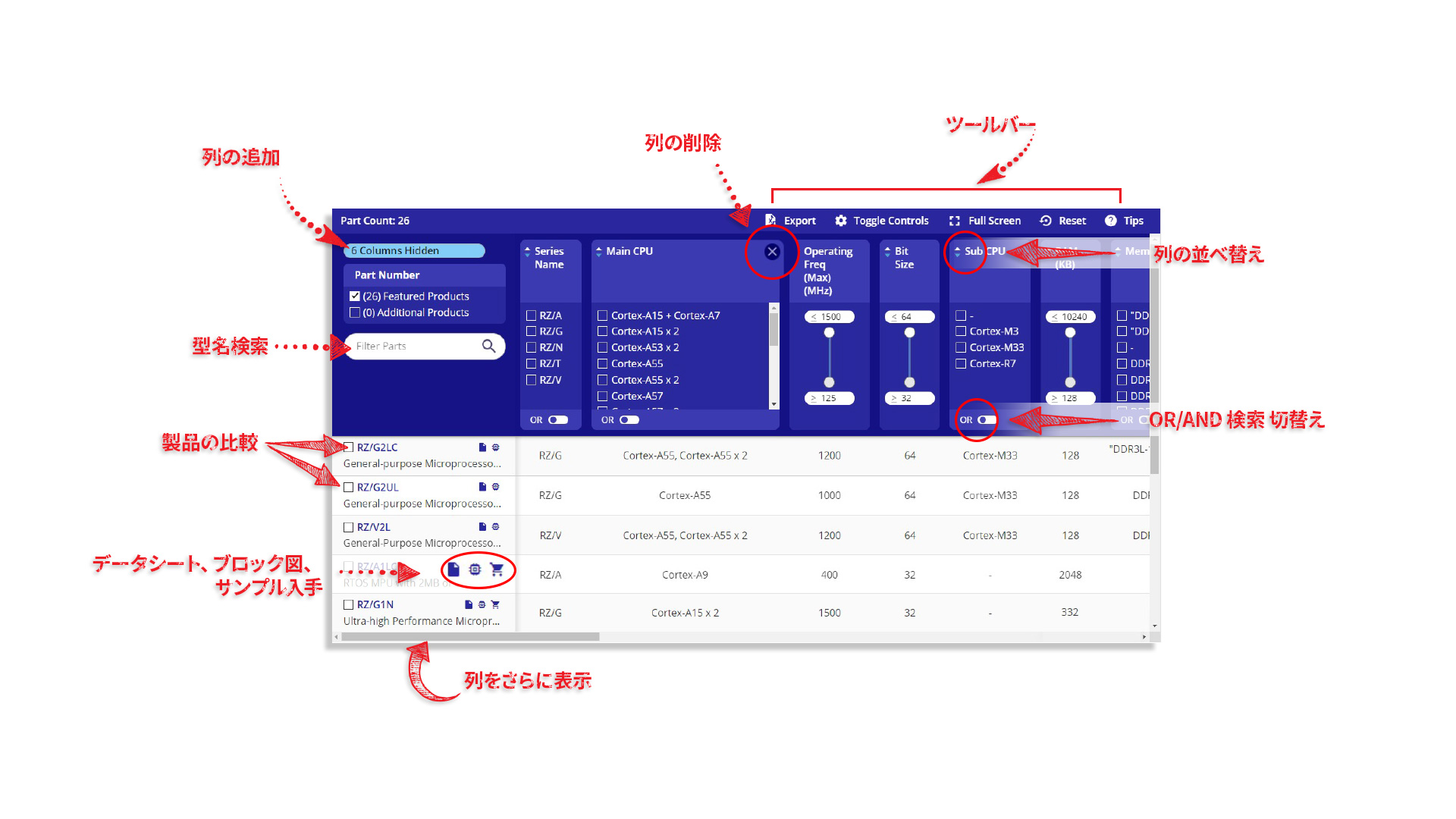
Tips for Using This Parametric Table:
- Hide Filters button in header: Collapse or expands filters
- Column sort buttons in header: Sort Column alphabetically / numerically descending or ascending
- Reset button in header: Reset all filters to the page default
- Full Screen button in header: Expand the table to full screen view (user must close out of full screen before they can interact with rest of page)
- Export button in header: Export the filtered results of the table to an Excel document
- Filter parts search bar in header: Type to filter table results by part number
- Hide column button in column headers: Select to hide columns in table
- AND / OR toggle switches in header: Toggles the logic of this particular filter to be “AND” or “OR” logic for filtering results
- Multiselect checkboxes at beginning of each row in table: Select these checkboxes to compare products against each other
- Document icon next to product name in row: View the featured document for this product
- Chip icon next to the right of the document icon in row: View the block diagram for this product
- Cart icon to the right of the chip icon: Indicates that samples are available for this product