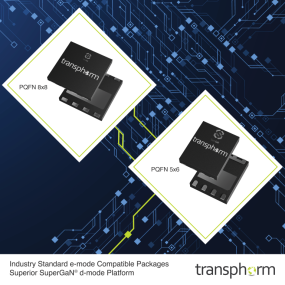
GOLETA, Calif. — Transphorm, Inc. (Nasdaq: TGAN)—a pioneer in and global supplier of high reliability, high performance gallium nitride (GaN) power conversion products—announced today the availability of six (6) surface mount devices (SMDs) available in Industry Standard PQFN 5x6 and 8x8 packages. These SMDs deliver the reliability and performance advantages offered by Transphorm's patented SuperGaN® d-mode two-switch normally-off platform in the package configurations typically used by competitive e-mode GaN devices. As a result, these six devices can easily serve as a first design source or as pin-to-pin drop-in replacements and/or secondary sources for e-mode GaN solutions.
For power systems that require additional thermal performance from the SuperGaN platform, Transphorm also offers SMDs in optimized Performance packages. All Transphorm devices offer easy designability and drivability regardless of packaging given the d-mode configuration's use of a low-voltage Silicon MOSFET paired with the GaN HEMT. This platform configuration also allows for the use of standard, off-the-shelf controllers and/or drivers adding to the Transphorm portfolio's superior drivability and designability.
"Transphorm continues to produce a strong GaN device portfolio, one that covers the widest power spectrum today. We've solidified our low power strategy with the release of these Industry Standard packages, which follow the recently announced SiP developed with Weltrend Semiconductors," said Philip Zuk, Senior Vice President of Business Development and Marketing, Transphorm. "Customers now have a choice of how they can tap into the advantages of SuperGaN whether it be through Performance packages, pin-to-pin e-mode compatible Industry Standard packages, or a System-in-Package."
SuperGaN Drop-In Replacement Advantages
Replacing e-mode devices with SuperGaN d-mode FETs has proven to deliver higher performance and lower operating temperature through lower conduction losses, resulting in longer lifetime reliability. This is due to the fundamental intrinsic superiority of the d-mode GaN normally-off device vs. the e-mode GaN normally-off device. One example of such validation can be found in a recent head-to-head comparison wherein 50 mΩ e-mode was replaced by 72 mΩ SuperGaN technology in a 280 W gaming laptop charger: https://bit.ly/diraztbISP.
In the charger analysis, the SuperGaN FETs operated at the controller's output voltage range (whereas e-mode had to level shift) with cooler temperatures. The SuperGaN temperature coefficient of resistance (TCR) is approximately 25 percent lower than that of e-mode, contributing to the lower conduction losses. Additionally, the peripheral component count was reduced by 20%, suggesting a lower BOM cost.
Industry Standard SMD Portfolio
Transphorm's Industry Standard PQFN device list follows:
| Part | RDS(on) mΩ | Package |
|---|---|---|
| TP65H070G4LSGB | 72 | PQFN88 |
| TP65H150BG4JSG | 150 | PQFN56 |
| TP65H150G4LSGB | 150 | PQFN88 |
| TP65H300G4JSGB | 240 | PQFN56 |
| TP65H300G4LSGB | 240 | PQFN88 |
| TP65H480G4JSGB | 480 | PQFN56 |
Key features shared across devices include:
- JEDEC qualified
- Dynamic RDS(on)eff production tested
- Market-leading robustness with wide gate safety margins and transient over-voltage capabilities
- Very low QRR
- Reduced crossover loss
Target Applications
The 72 mΩ FET is optimally designed for use in datacom, broad industrial, PV inverter, servo motor, computing systems, and general consumer applications.
The 150, 240, and 480 mΩ FETs are optimally designed for use in power adapter, low power SMPS, lighting, and low power consumer applications.
Availability
All Industry Standard devices are currently sampling and can be requested here: https://www.transphormusa.com/en/products/#sampling.
About Transphorm
Transphorm, Inc., a global leader in the GaN revolution, designs and manufactures high performance and high reliability GaN semiconductors for high voltage power conversion applications. Having one of the largest Power GaN IP portfolios of more than 1,000 owned or licensed patents, Transphorm produces the industry's first JEDEC and AEC-Q101 qualified high voltage GaN semiconductor devices. The Company's vertically integrated device business model allows for innovation at every development stage: design, fabrication, device, and application support. Transphorm's innovations move power electronics beyond the limitations of silicon to achieve over 99% efficiency, 50% more power density and 20% lower system cost. Transphorm is headquartered in Goleta, California and has manufacturing operations in Goleta and Aizu, Japan. For more information, please visit www.transphormusa.com. Follow us on Twitter @transphormusa and WeChat @ Transphorm_GaN.
The SuperGaN mark is a registered trademark of Transphorm, Inc. All other trademarks are the property of their respective owners.
The content in the press release, including, but not limited to, product prices and specifications, is based on the information as of the date indicated on the document, but may be subject to change without prior notice.
