Our Targets
In our previous blog, we explained the technical background of Power over Data Line (PoDL). In this blog, we are sharing information about a flexible and easy-to-use reference design supporting most of the IEEE features and power classes. Such reference design should be capable of hosting a simple application and evaluating power delivery features. In addition, we were targeting to support a use case where we connect a classical radar sensor with a CSI2 interface to an Ethernet network. Both use cases are available as a Renesas Winning Combination reference design. More information about the radar use case can be found on our Satellite Radar System for AD/ADAS page.
A wide variety of applications can be built on these modules by the interfaces provided by the RH850/F1KM-S4, the FPGA, and the exposed connector interfaces.
Realization
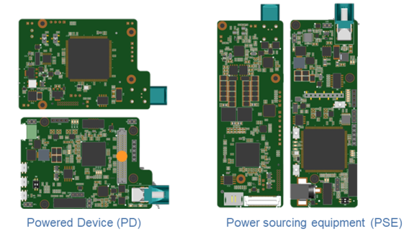
Although from the block diagram level Power Sourcing Equipment (PSE) and Powered Device (PD) look very similar, the details, especially for the analog and power portions, are quite different. The PD and PSE design can be grouped into four parts:
- Ethernet PHY
This part includes the Ethernet PHY, the common mode chokes, and the coupling capacitors. PoDL is strongly independent of PHY, so we’ve chosen a standard PHY that operates in 100BASE-T1 and 1000BASE-T1. For the coupling, capacitors with higher dielectric strength are required to sustain a higher PoDL voltage level. This part is identical between PD and PSE. - Application zone
This part includes the RH850/F1KM-S4 Microcontroller, expansion connector, and a Lattice FPGA interfacing with the other modules. Here the implementation is also identical between PD and PSE. - PoDL
Here the PoDL-specific functions are located. This part is different between PD and PSE and will be explained in detail in the following sections. - System power
In this part, the operation voltage levels are generated based on external supply or injected PoDL voltage.
Automotive-grade products were certainly one of the selection criteria but not mandatory for this reference design. However, many components are qualified for automotive use cases or have variants for this application area.
Power sourcing equipment
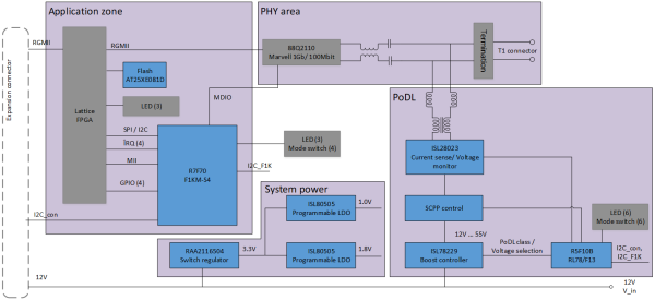
In the multi-purpose use case, the RH850/F1KM-S4 is hosting the application, taking care of configuring the PHY, and instructing the RL78/F13 via I2C to control the PoDL function. The FPGA can host some custom function or, as in the radar use case, switches, the RGMII between PHY, RH850/F1KM-S4 and expansion connector. The connector holds an I2C interface for custom expansions. The detailed block diagram of the PSE is shown in Figure 2.
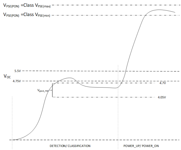
The PoDL functionality, i.e. voltage level creation, current sensing, voltage monitoring, and Serial Communication Classification Protocol (SCCP) is controlled by the RL78/F13. A small firmware has the specified state machine implemented [1] and controls the ISL78229, voltage monitor part, and current sense amplifier depending on the state of the PoDL FSM. In the SIGNATURE DETECTION state, the PSE must supply an open circuit voltage (V_OC = 4.75V – 5.5V) and detect a valid PD when the probing voltage (V_good_PSE) is in the range of 4.05V and 4.7V for a specific time. During this probing phase, the PD must draw a current (I_valid) in the range of 9mA to 16mA. In this state, SCCP can be used to get information about the power class of the connected PD. In case the detection is successful the PSE can increase the output level V_PSE(PON) to the selected PoDL voltage level. Figure 3 shows the described behavior in a timing diagram. The optional classification phase using SCCP is likely to be skipped in engineered networks and not used in this reference design but prepared for usage. In our case, the output level is selectable by switches and covers all PoDL classes. The user must ensure that PSE and PD have the same settings. With the devices selected for this reference design, we support PoDL classes 0 to 15. Most applicable for automotive are the classes 0 to 9 (12V, 24V, and 48V).
The power supply is shut down in case the output limits are exceeded (I_LIM) as a safety measure to prevent overload of the PSE. In case the consumed current drops below I_HOLD (2.5mA to 10mA) the PSE either switches off or goes into sleep mode where V_Sleep (3.15V to 3.575V) is supplied. In this state, the PD can wake up the PSE by drawing more than 10mA the process restarts with SIGNATURE DETECTION.
In the multi-purpose use case, the RH850/F1KM-S4 can host a full application and make use of the rich feature set of this microcontroller. In the reference design, a small example application is available that can issue a “sleep” and “shut down” command to the connected powered device over Ethernet. Using the I2C interface the RH850/F1KM-S4 can manage the RL78/F13 for mode transitions and extended monitoring functionality.
The FPGA does not play a major role in the PSE in both use cases. The primary function is to switch and convert the Ethernet RGMII/MII to connect to the Ethernet PHY. Customers using this evaluation platform can add here custom logic.
Powered device
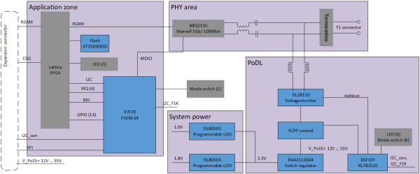
The block level structure of the PD is very similar to the PSE consisting of an RH850/F1KM-S4 to host an application, an RL78/G10 to control the PoDL function and an FPGA for custom logic or, as in the radar use case, the conversion function to Ethernet. The detailed block diagram of the PD is shown in Figure 4.
On the RL78/G10 runs a small firmware implementing the required state diagram for a PD. In SLEEP mode all devices and regulators are in power off state. When the PSE side applies the detection voltage level the PD forces a valid signature detection current with a Z-Diode. Device classification using SCCP is done under the control of the RL78/G10. When SCCP is operated, the supply voltage is not available for the RL78/G10 during the low phases of the protocol. The ultra-low power consumption of the RL78/G10 makes large capacitors unnecessary and helps to keep the current flowing into the PD within the specified bands. When the operation voltage level is detected at the voltage monitor, the PD wakes up and enters normal operation. A voltage level below the specified operation voltage causes the device to move back into PD_SLEEP. Upon fault detection (overcurrent) the PD disconnects from the power source by itself (Figure 5).
Through I2C communication, the RH850/F1KM-S4 can instruct the RL78/G10 to go back into the DISCONNECT state and query the operation state. Those state transitions are implemented in the reference design by Ethernet communication between PSE and PD using a custom UDP protocol. This implementation can be a starting point for more complex applications. In the radar use case, the microcontroller is also responsible for managing the radar MMIC. Based on commands received over the Ethernet channel, the MMIC is configured and managed. Because the RH850/F1KM-S4 is only capable of communication using 100Mbit Ethernet, an Ethernet MAC is implemented in the FPGA to handle the 1Gbit communication and exchange the data between the RH850/F1KM-S4 in both directions. In addition, the FPGA is programmed to perform radar data to Ethernet conversion. Firmware on the RH850/F1KM-S4 is available for the MMIC configuration, configuration of FPGA content, and Ethernet communication. For a multi-purpose use case, the FPGA can hold some custom logic, bridge the RGMII to the connector, or switch the Ethernet interface to the RH850/F1KM-S4. When using the RH850/F1KM-S4, the link speed is limited to 100Mbit/s.
Key components
RL78 microcontroller
Controlling the PD and PSE functions can be done easiest with the RL78/F13 microcontroller with the industry's lowest level of consumption current. These MCUs have a built-in CAN module and LIN module for automotive interfaces; and in addition to the functional safety features, a RAM ECC function, PLL lock function, port output state monitoring, stack overflow detection, dedicated WDT oscillator, and more features have also been added. Since a more highly reliable system can be built, these microcontrollers can be used for industrial applications and of course automotive applications. [4]
RH850/F1KM-S4 microcontroller
One of the centerpieces in this design is the RH850/F1KM-S4 microcontroller which is designed for automotive electrical body applications. The CAN FD, 100Mbit Ethernet, LIN, and other standard communication interfaces have been added to connect to other networking devices. In this reference design, only Ethernet, SPI, and I2C are exposed for external connections. [4]
ISL78229 synchronous boost controller
One of the targets for the general use case is to support all power classes and to generate the required injection voltage from a typical 12V connector. The ISL78229 is an automotive grade (AEC-Q100 Grade 1), 2-phase 55V synchronous boost controller that simplifies the design of high-power boost applications. It integrates strong half-bridge drivers, an analog/digital tracking input, comprehensive protection functions, and a PMBus interface for added control and telemetry. The ISL78229 enables a simple, modular design for systems requiring power and thermal scalability. [4]
RAA2116504 buck-boost controller
Having a wide range of PoDL voltages, the input voltage regulator on the PD side must be capable of handling voltages up to 60V. The RAA2116504 is an integrated 60V, 5A synchronous buck regulator with adjustable switching frequency from 200kHz up to 2.5MHz. It supports the required wide input voltage range from 4.5V to 60V and adjustable output voltage. [4]
Lattice Crosslink NX
Lattice CrossLink™-NX FPGAs [5] deliver the best-in-class low power consumption, small form factor, reliability, and performance that developers need to create innovative embedded vision and AI solutions for the Compute, Industrial, Automotive, and Consumer markets. The CrossLink-NX family is based on the Lattice Nexus™ platform, the industry’s only low power FPGA platform using a 28nm fully-depleted silicon-on-insulator (FD-SOI) manufacturing process. The Nexus platform features a Lattice-designed FPGA fabric architecture optimized for low power operation in a small form factor. [6]
Summary
The PoDL reference design from Renesas provides an easy-to-start platform for customers evaluating PoDL in various use cases. The power delivery service over single-pair Ethernet allows for a significant reduction of implementation cost into the overall system, reduction of cabling and mounting efforts, and centralized power management.
References:
[1] The Art of Networking (Series 10): Power over Data Line is ready to use
[2] Satellite Radar System for AD/ADAS
[3] IEEE 802.3-2022
[4] Renesas Electronics Corporation
[5] Lattice CrossLink™-NX


