概要
説明
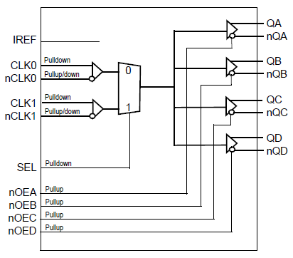
The 831724I is a high-performance, differential HCSL clock/data multiplexer and fanout buffer. The device is designed for the multiplexing and fanout of high-frequency clock and data signals. The device has two differential, selectable clock/data inputs. The selected input signal is distributed to four low-skew differential HCSL outputs. Each input pair accepts HCSL, LVDS, LVPECL and SSTL levels. The 831724I is characterized to operate from a 3.3V power supply. Guaranteed input, output-to-output and part-to-part skew characteristics make the 831724I ideal for those clock and data distribution applications demanding well-defined performance and repeatability. The 831724I supports the clock multiplexing and distribution of PCI Express (2.5 Gb/s) and Gen 2 (5 Gb/s) clock signals. The device is a member of the family of High Performance Clock Solutions from IDT.

特長
-
2:1 differential clock/data multiplexer with fanout
-
Two selectable, differential inputs
-
Each differential input pair can accept the following levels: HCSL, LVDS, LVPECL
-
Four differential HCSL outputs
-
Maximum input/output clock frequency: 350MHz
-
Maximum input/output data rate: 700Mb/s (NRZ)
-
LVCMOS interface levels for all control inputs
-
PCI Express Gen 1,2,3 jitter compliant
-
Input skew: 165ps (maximum)
-
Output skew: 175ps (maximum)
-
Part-to-part skew: 450ps (maximum)
-
Full 3.3V supply voltage
-
Available in lead-free (RoHS 6) package
-
-40°C to 85°C ambient operating temperature
製品比較
アプリケーション
設計・開発
モデル
ECADモデル
[製品選択]テーブル内の製品名をクリックするとSamacSysが提供する回路図シンボル、PCBフットプリント、3D CADモデルがご確認いただけます。 お探しのシンボルやモデルが見つからない場合、Webサイトから直接リクエストできます。

製品選択
適用されたフィルター