概要
説明
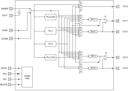
The 5V49EE503 is a programmable clock generator intended for high performance data-communications, telecommunications, consumer, and networking applications. There are four internal PLLs, each individually programmable, allowing for four unique non-integer-related frequencies. The frequencies are generated from a single reference clock. The reference clock can come from one of the two redundant clock inputs. Automatic or manual switchover function allows any one of the redundant clocks to be selected during normal operation. The 5V49EE503 is in-system, programmable and can be programmed through the use of I2C interface. An internal EEPROM allows the user to save and restore the configuration of the device without having to reprogram it on power-up. Each of the four PLLs has an 7-bit reference divider and a 12-bit feedback divider. This allows the user to generate four unique non-integer-related frequencies. The PLL loop bandwidth is programmable to allow the user to tailor the PLL response to the application. For instance, the user can tune the PLL parameters to minimize jitter generation or to maximize jitter attenuation. Spread spectrum generation and/or fractional divides are allowed on two of the PLLs. There are a total of four 8-bit output dividers. The outputs are connected to the PLLs via a switch matrix. The switch matrix allows the user to route the PLL outputs to any output bank. This feature can be used to simplify and optimize the board layout. In addition, each output's slew rate and enable/disable function is programmable.
特長
- Four internal PLLs
- Internal non-volatile EEPROM
- Fast (400kHz) mode I2C serial interface
- Input frequency range: 1 MHz to 200 MHz
- Output frequency range: 4.9 kHz to 200 MHz
- Reference crystal input with programmable linear load capacitance - Crystal frequency range: 8 MHz to 50 MHz
- Each PLL has a 7-bit reference divider and a 12-bit feedback-divider
- 8-bit output-divider blocks
- Fractional division capability on one PLL
- Two of the PLLs support spread spectrum generation capability
- I/O Standards: - Outputs - 3.3 V LVTTL/ LVCMOS - Inputs - 3.3 V LVTTL/ LVCMOS
- Programmable slew rate control
- Programmable loop bandwidth
- Programmable output inversion to reduce bimodal jitter
- Redundant clock inputs with auto and manual switchover options
- Individual output enable/disable
- Power-down mode
- 3.3V core VDD
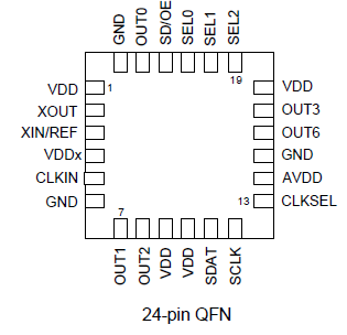
- Available in VFQFPN package
- -40 to +85 C Industrial Temp operation
製品比較
アプリケーション
設計・開発
ソフトウェア/ツール
モデル
ECADモデル
[製品選択]テーブル内の製品名をクリックするとSamacSysが提供する回路図シンボル、PCBフットプリント、3D CADモデルがご確認いただけます。 お探しのシンボルやモデルが見つからない場合、Webサイトから直接リクエストできます。

製品選択
適用されたフィルター
ビデオ&トレーニング
Description
Transcript


