概要
説明
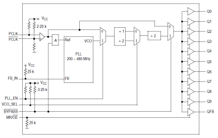
The MPC9658 utilizes PLL technology to frequency lock its outputs onto an input reference clock. Normal operation of the MPC9658 requires the connection of the QFB output to the feedback input to close the PLL feedback path (external feedback). With the PLL locked, the output frequency is equal to the reference frequency of the device and VCO_SEL selects the operating frequency range of 50 to 125 MHz or 100 to 250 MHz. The two available post-PLL dividers selected by VCO_SEL (divide-by-2 or divide-by-4) and the reference clock frequency determine the VCO frequency. Both must be selected to match the VCO frequency range. The internal VCO of the MPC9658 is running at either 2x or 4x of the reference clock frequency. The MPC9658 has a differential LVPECL reference input along with an external feedback input. The MPC9658 is ideal for use as a zero delay, low skew fanout buffer. The device performance has been tuned and optimized for zero delay performance. The PLL_EN and BYPASS controls select the PLL bypass configuration for test and diagnosis. In this configuration, the selected input reference clock is bypassing the PLL and routed either to the output dividers or directly to the outputs. The PLL bypass configurations are fully static and the minimum clock frequency specification and all other PLL characteristics do not apply. The outputs can be disabled (high-impedance) and the device reset by asserting the MR/OE pin. Asserting MR/OE also causes the PLL to loose lock due to missing feedback signal presence at FB_IN. Deasserting MR/OE will enable the outputs and close the phase locked loop, enabling the PLL to recover to normal operation. The MPC9658 is fully 3.3 V compatible and requires no external loop filter components. The inputs (except PCLK) accept LVCMOS except signals while the outputs provide LVCMOS compatible levels with the capability to drive terminated 50 ? transmission lines. For series terminated transmission lines, each of the MPC9658 outputs can drive one or two traces giving the devices an effective fanout of 1:16. The device is packaged in a 7x7 mm2 32-lead LQFP package.
特長
- Low based low-voltage clock generator
- Supports zero-delay operation
- 3.3 V power supply
- Generates clock signals up to 250 MHz
- Maximum output skew of 120 ps
- Differential LVPECL reference clock input
- External PLL feedback
- Drives up to 20 clock lines
- 32-lead LQFP packaging
- 32-lead Pb-free Package Available
- Pin and function compatible to the MPC958
製品比較
アプリケーション
設計・開発
モデル
ECADモデル
[製品選択]テーブル内の製品名をクリックするとSamacSysが提供する回路図シンボル、PCBフットプリント、3D CADモデルがご確認いただけます。 お探しのシンボルやモデルが見つからない場合、Webサイトから直接リクエストできます。

製品選択
適用されたフィルター
