概要
説明
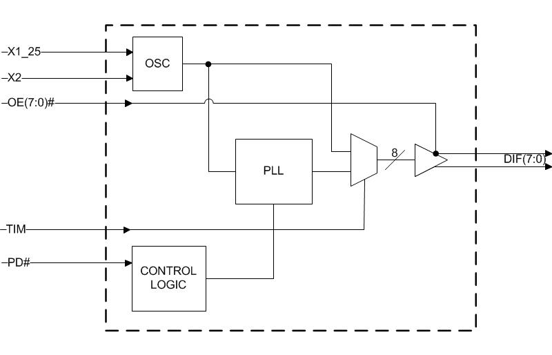
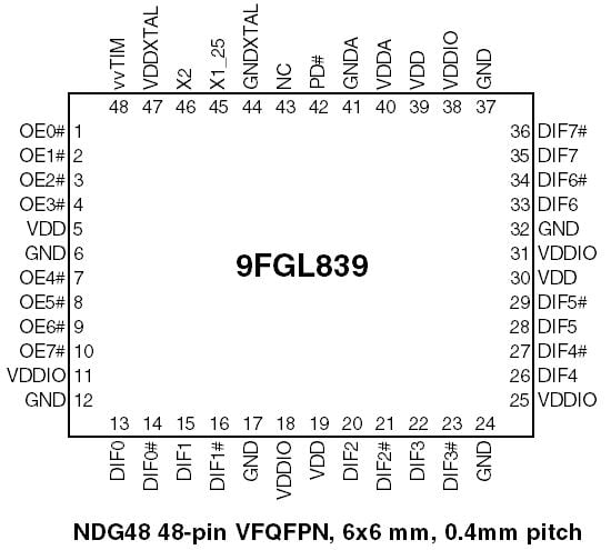
The 9FGL839 is an 8-output differential synthesizer for PCI Express Gen 1, Gen 2, and Gen 3 applications. It has integrated terminations providing direct connection to 100Ω transmission lines and saving 32 resistors compared to standard HCSL outputs. The 9FGL839 supports common, data, and Separate Reference no-Spread (SRnS) PCIe clock architectures.
特長
- Integrated terminations; save 32 resistors compared to standard HCSL outputs
- LP-HCSL outputs; support separate VDDIO rail and 130mW typical power consumption
- 8 OE# pins; hardware control of each output
- 25MHz crystal input; exact synthesis
- 100MHz operation; supports PCIe and SATA applications
- VDDIO; allows outputs to run from lower voltage rail to save power
- OE# pins have 1.5V high input threshold; direct interface to 1.8V to 3.3V systems
- < 130mW power consumption (typical)
- Cycle-to-Cycle jitter < 50ps
- Output-to-Output skew < 100ps
- PCIe Gen 2 phase jitter < 3.0ps RMS
- PCIe Gen 3 phase jitter < 1.0ps RMS
- PCIe Gen 3 SRnS clock phase jitter < 0.7ps RMS
製品比較
アプリケーション
設計・開発
モデル
ECADモデル
[製品選択]テーブル内の製品名をクリックするとSamacSysが提供する回路図シンボル、PCBフットプリント、3D CADモデルがご確認いただけます。 お探しのシンボルやモデルが見つからない場合、Webサイトから直接リクエストできます。

Processing table
| VFQFPN | 48 | I | Yes | Tray | ||
| VFQFPN | 48 | I | Yes | Reel | ||
| VFQFPN | 48 | C | Yes | Tray | ||
| VFQFPN | 48 | C | Yes | Reel |

Tips for Using This Parametric Table:
- Hide Filters button in header: Collapse or expands filters
- Column sort buttons in header: Sort Column alphabetically / numerically descending or ascending
- Reset button in header: Reset all filters to the page default
- Full Screen button in header: Expand the table to full screen view (user must close out of full screen before they can interact with rest of page)
- Export button in header: Export the filtered results of the table to an Excel document
- Filter parts search bar in header: Type to filter table results by part number
- Hide column button in column headers: Select to hide columns in table
- AND / OR toggle switches in header: Toggles the logic of this particular filter to be “AND” or “OR” logic for filtering results
- Multiselect checkboxes at beginning of each row in table: Select these checkboxes to compare products against each other
- Document icon next to product name in row: View the featured document for this product
- Chip icon next to the right of the document icon in row: View the block diagram for this product
- Cart icon to the right of the chip icon: Indicates that samples are available for this product
ビデオ&トレーニング
PCIe Clocking Architectures (Common and Separate)
This is the first video in our PCIe series. In this video, we define PCIe architectures, focusing on common and separate clock architectures. Watch the rest of the video series below where Ron will cover the impact of different timing architectures.
Watch the Video Series Below
Video List