概要
説明
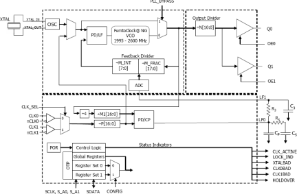
The 840N202I is a highly flexible FemtoClock® NG general purpose, low phase noise Frequency Translator / Synthesizer with alarm and monitoring functions suitable for networking and communications applications. It is able to generate any output frequency in the 1MHz - 250MHz range (see Table 3 for details). A wide range of input reference clocks and a range of low- cost fundamental mode crystal frequencies may be used as the source for the output frequency. The 840N202I has three operating modes to support a very broad spectrum of applications: Frequency Synthesizer , High-Bandwidth Frequency Translator and a Low-Bandwidth Frequency Translator.
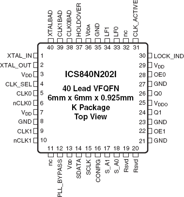
This device provides two factory-programmed default power-up configurations burned into One-Time Programmable (OTP) memory. The configuration to be used is selected by the CONFIG pin. The two configurations are specified by the customer and are programmed by IDT during the final test phase from an on-hand stock of blank devices. The two configurations may be completely independent of one another.
To see other devices in this product family, visit the Universal Frequency Translators page.
特長
- Fourth generation FemtoClock® NG technology
- Universal Frequency Translator/Frequency Synthesizer
- Two LVCMOS/LVTTL outputs
Both outputs may be set to use 2.5V or 3.3V output levels
Programmable output frequency: 1.0MHz to 250MHz - Two differential inputs support the following input types: LVPECL, LVDS, LVHSTL, HCSL
- Input frequency range: 8kHz - 710MHz
- Crystal input frequency range: 16MHz - 40MHz
- Two factory-set register configurations for power-up default state
Power-up default configuration pin or register selectable
Configurations customized via One-Time Programmable ROM
Settings may be overwritten after power-up via I2C
I2C Serial interface for register programming - RMS phase jitter at 125MHz, using a 40MHz crystal (12kHz - 20MHz): 616fs (typical), Low Bandwidth Mode (FracN)
- Output supply voltage modes:
VDD/VDDA/VDDO
3.3V/3.3V/3.3V
3.3V/3.3V/2.5V
2.5V/2.5V/2.5V - -40°C to 85°C ambient operating temperature
- Lead-free (RoHS 6) packaging
製品比較
アプリケーション
設計・開発
モデル
ECADモデル
[製品選択]テーブル内の製品名をクリックするとSamacSysが提供する回路図シンボル、PCBフットプリント、3D CADモデルがご確認いただけます。 お探しのシンボルやモデルが見つからない場合、Webサイトから直接リクエストできます。

製品選択
適用されたフィルター
ビデオ&トレーニング
ニュース&ブログ
| Benefits of a Point-of-Use Clock for Jitter Optimization | ブログ | 2021年4月27日 |

