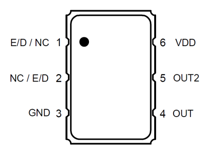
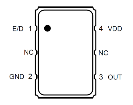
概要
説明
XUは、400fs以下の位相ジッタを持つ水晶ベースのPLLクロックオシレータで、幅広い周波数、入力電圧、出力タイプに対応しています。 これらのデバイスは、3つの異なる電源で動作するように設計されており、豊富なパッケージサイズと温度グレードが用意されています。
特許取得済みのワンタイムプログラム(OTP)により、メモリの保存期間を無限にすることができ、XUデバイスは16kHzから1500MHzまでの出力周波数を、1Hzという低い精度で生成するようにプログラムすることが可能です。 このファミリのデバイスは構成機能が可能なため、サンプル品から大量生産品まで短納期で提供することができます。
特長
- 周波数範囲: 0.016MHz ~ 1500MHz
- 出力タイプ: LVDS, LVPECL, HCSL, LVCMOS
- 電源電圧: 1.8V, 2.5V または 3.3V
- 位相ジッタ (12kHz ~ 20MHz): 300fs typical (400fs max)
- パッケージ・オプション:
- 5.0 x 3.2x 1.2 mm
- 7.0 x 5.0 x 1.3 mm
- 周波数安定性: ± 20ppm ± 25ppm, ± 50ppm, or ± 100 ppm
- 動作温度範囲: -20°C ~ +70°C
- 周波数安定性: ± 25ppm, ± 50ppm, または ± 100 ppm
- 動作温度範囲: -40°C ~ +85°C
- 周波数安定性: ± 50ppm, または ± 100 ppm
- 動作温度範囲: -40°C ~ +105°C
製品比較
アプリケーション
ドキュメント
|
|
|
|
|---|---|---|
| 分類 | タイトル | 日時 |
| データシート | PDF 340 KB | |
| 概要 | PDF 526 KB | |
| 概要 | PDF 525 KB | |
| ガイド | PDF 7.95 MB | |
| ガイド | PDF 321 KB | |
| アプリケーションの概要 | PDF 686 KB | |
| ガイド | XLS 3.38 MB | |
| 製品変更通知 | PDF 662 KB | |
8件
|
||
設計・開発
モデル
ECADモデル
[製品選択]テーブル内の製品名をクリックするとSamacSysが提供する回路図シンボル、PCBフットプリント、3D CADモデルがご確認いただけます。 お探しのシンボルやモデルが見つからない場合、Webサイトから直接リクエストできます。

製品選択
適用されたフィルター
ビデオ&トレーニング
IDT provides a brief overview of the timing solutions optimized for various configurations using the NXP (Freescale) QorIQ / Layerscape processors.
Presented by Ron Wade, PCI Express timing expert. For more information about IDT's timing solutions, visit www.IDT.com/go/clocks.
TRANSCRIPT
So, hi there, this is Ron Wade again and we're going to be talking about timing solutions that IDT has for NXP's QorIQ and Layerscape CPU. And in the middle here, what I've drawn, in the middle of the box here, is what I refer to as our all-in-one solutions. These are single chips that may have all the clocks you need to build your system around the NXP CPUs. So, the three parts I have listed here are the 6P49V205, the 5P49V5907, and 5P49V5908. These provide a mix of the clocks that were needed over here for the CPU cores and SerDes clocks, and they're all on a single chip. If these suit your needs, these are ideal, these are the smallest core footprint parts to use.
The other approach besides all-in-one is the building block approach, and I'm going to start over here on the left side with the CPU clocks and the memory controller. For this solution over here, we have the 5P49V5901, or it could be a 6901, depending on your requirements. And, this guy has the most flexibility as far as programming up any combination of DDR clock or CPU clock that you want, as well as the 24 MHz USB clock and a 125 MHz clock.
If you're using the Layerscape CPU with the reduced oscillator mode where you have the 100 MHz non-spread clock coming in, you might want to consider the 9FGV0 series or the 9FGL0 series. These are very high-performance PCI Express clock generators, the V being a 1.8 volt part and the L being a 3.3 volt part that are available. The terminations are integrated, they're very low power and they also have some extra copies in case SerDes is a PCI Express SerDes. So, this is the ideal solution if you want to go building block over here.
And then for the SerDes clocks, we've got the 125 MHz differential for Gigabit Ethernet, the 156 MHz for 10 gig, and the 100 MHz for PCIe. We have again a different set of flavors we can go with. We have the 5P49V6901, which is a better performing, lower phase jitter version of the 5901 over here. This guy's ideal if you have a mix of these SerDes frequencies in your design. If you're in a homogeneous environment, for instance, where everything's PCI Express or everything is 125 MHz, then you could use the 9FGV parts, or I'll use an output from over there, over on this side for the 100 MHz output, or you could use these guys programmed up to be 125 as well. Or if you've got a 125 coming from over there, you can use one of the 9DVD buffers which are the 1.8V buffers to fan that out. Likewise, we have similar parts with 3.3-volt power supplies, if that's what you prefer. The 9FGL0 series, it should give you the 100 to the 125, and the 9DVL0 series which can provide a fanout buffer for any of these three frequencies.
So, that's an overview of the timing solutions for NXP's QorIQ and Layerscape CPUs. This is Ron Wade at IDT again. Thanks for watching and see you next time.


