Calculators for Estimating Noise Amplitudes & Selecting the Best Data Converter

Renesas' Thermal Noise Calculator (TNC) and Effective Number of Bits (ENOB) Calculator help analyze noise that is present in semiconductor devices as well as noise due to signal processing in data converters.

Using the calculators, you can enter or find all parameters. The calculators also offer an indication of consistent parameters, validation to prevent illegal entries, and import, export and graphing functionality.

System Requirements

  • Windows 7® or Windows® 8
  • File Size: 30MB

Thermal Noise Calculator

The Thermal Noise Calculator aids in the analysis of thermal noise found in resistors and other noise sources. The TNC finds the noise voltage generated by any device if the white noise spectral density and 1/f corner frequency are known.
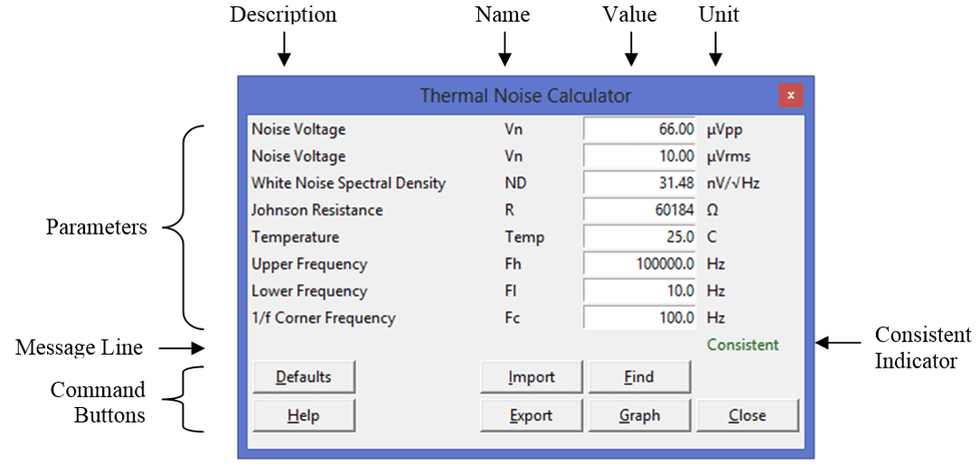
Thermal Noise Calculator

Parameters

  • Noise Voltage, Vn, in μVpp or μVrms
  • White Noise Spectral Density, ND, in nV/√Hz
  • Johnson Resistance, R, in Ω
  • Temperature, T, in °C
  • Upper Frequency, Fh, in Hz
  • Lower Frequency, Fl, in Hz
  • 1/f Corner Frequency, Fc, in Hz

Effective Number of Bits Calculator

ENOB is an AC specification and is synonymous with Signal to Noise and Distortion. The ENOB Calculator aids in the design and analysis of data converter application circuits. It calculates the effective number of bits of an ideal data converter.
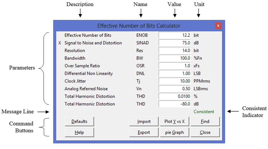
Effective Number of Bits Calculator

Parameters

  • Effective Number of Bits, ENOB, in bits
  • Signal to Noise and Distortion, SINAD, in dB
  • Resolution, N, in bits
  • Bandwidth, BW, in % of the Nyquist frequency, or Over Sample Ratio, OSR, as a multiple of the sample frequency
  • Average Differential Nonlinearity, DNL, in LSB
  • Clock Jitter, Tj, in PPMrms of the clock period
  • Analog Referred Noise, Vn, in LSBrms
  • Total Harmonic Distortion, THD, in % or dB

ドキュメント

分類 タイトル 日時
ガイド PDF 445 KB
プレゼンテーション PDF 2.35 MB
2件

ダウンロード

分類 タイトル 日時
ライブラリ ログインしてダウンロード EXE 27.63 MB
ライブラリ ログインしてダウンロード EXE 28.78 MB
2件

ビデオ

Understanding Noise in the Signal Chain Webinar

Learn more about how noise affects the performance of the signal chain and how to use Intersil's tools to help analyze noise that is present in semiconductor devices as well as noise due to signal processing in data converters.

Transcript

Understanding Noise in the Signal Chain

This is a short course on one of the most important, and in my opinion least understood, aspects of circuit and systems design – and that is, noise and it effects on the performance of signal chain.

In this course you will be learning three things:

  1. What is noise and how it is specified at the component level
  2. How this noise effects the performance of a signal chain
  3. How to select components based on signal chain requirements

What is meant by a signal chain?

A signal chain is any series of components that processes a signal from input to output. It can include the components shown in the diagram, but can also include filters, mixers, voltage regulators, switches, sample and holds, any manor of DSP, etc.

Anything in a circuit that influences a signal can be considered a part of a signal chain.

What is Noise?

Noise is any electrical phenomenon that is unwelcomed in the signal chain.

It can have it origins external or internal to the chain. If it is external, it is interference.

In this course will focus on the internal sources. These come from two places.

  1. Noise that is present in all semiconductor devices in general
  2. Noise due to signal processing in data converters in particular

Noise in Semiconductor Devices

We begin by looking at noise that is common to semiconductor devices. We’ll look at how noise is specified, types of noise, how to read and interpret noise specifications in a datasheet, and how to take those specs and estimate noise amplitudes in various circuits and systems.

Noise is specified in two ways.

  1. Time domain: Amplitude
  2. Frequency domain: Spectral density

How Noise is Specified: Amplitude

Noise amplitude is specified in Vrms or Vpp. The important thing to understand about noise is that it’s random, and its amplitude follows a Gaussian distribution curve. I’ve shown that in this diagram.

The volts rms of the signal is the one sigma (σ) point on the curve. Vrms is an important unit because it represents the ability of a signal to deliver power to a load.

The peak amplitude is more difficult to define because in theory a random signal has no peak. If you wait long enough, it can have any amplitude. In practice a cresting factor of 6.6 is used. The value of 6.6 is somewhat arbitrary. It comes from fact that the amplitude of a random signal will exceeding +/-3.3 sigma 0.1% of the time. In other words, the probability of this occurring is 0.001. This is shown as the red area under the curve.

Bonus Facts:

P=(Vrms^2)/R

Vrms is equivalent to the DC value that yields the same power dissipation into a resistive load. It applies to any wave shape.

Common Cresting Factors

Here are some common cresting factors for your reference. In addition to the 6.6 for a random signal, as previously discussed, take note of the triangle wave with a cresting factor of root three. This will appear again when we discuss noise in data converters.

How Noise is Specified: Spectral Density

Noise is categorized as either White or Pink based on the shape of their spectrum.

White noise has a uniform spectral density, and Pink has one that increases with decreasing frequency. Because of this it is often called “1/f” noise”.

The names “Pink” and “White” are old terms that come from the optical world, where light that is made of multiple colors of equal brightness will appear white, and light that contains more of the lower frequency red spectrum will appear pink.

The noise spectral density at the boundaries of any device is the combination of all of the white and pink noise sources internal to it. This combined spectral density curve is shown in this diagram.

A noise spectral density curve is completely defined by two parameters, ND and Fc.

ND is the white noise density and Fc is the corner frequency. The corner frequency is the frequency at which the pink noise density equals the white noise density.


Types of Noise

In this section we look at the sources of white and pink noise.

Types of Noise: White Noise

We begin by looking at white noise sources.

As mentioned earlier, white noise has a uniform spectral density.

In the time domain, it looks like a fuzzy line. This is shown in the oscilloscope shot on the left where you can make out the Gaussian distribution of amplitude where it is denser (darker) in the center and thins out toward the peaks.

Thermal Noise

Thermal noise is the most common type of white noise. It’s found in all integrated and discreet resistors.

It’s caused by the random motion of electrons, due to heat, in the resistive medium.

It is important to note that this noise is only a function of temperature (T) and resistance (R), and does not require the flow of current. The only time it is not present is at absolute zero, or when there is absolutely no resistance.

So, every real resistor or conductor generates noise. It is inescapable.

Bonus Fact:

Because energy used to generate noise comes from heat, the power spectral density (PSD) is only a function of temperature, 4kT (W/Hz).

Shot Noise

Shot noise (also called Schottky noise) is another type of white noise. It got the name “Shot” because in an audio system, it sounded to somebody like the hissing or sputtering of a shot being fired from a shotgun.

This noise is generated whenever charge crosses a potential barrier, so it is found in all semiconductor devices such as diodes and transistors.

It’s caused by the fact that current flowing across a junction is not smooth, but is made of individual electrons arriving at random times due to electron-hole recombination.

Unlike thermal noise, shot noise density is only a function of current.

Bonus Fact:

q = 1.6*10^-19 C

Avalanche Noise

A third source of white noise is avalanche noise.

This noise is found in PN junctions operating in reverse breakdown mode, such as Zener diodes.

It’s caused by carriers developing sufficient energy to dislodge additional carriers through physical impact. This results in an avalanche of discrete carriers that produce a random fluctuation in current.

Like shot noise, avalanche noise requires the flow of current.

Types of Noise: Pink Noise

The second type of noise is pink noise. Pink noise is characterized by increasing spectral density at decreasing frequencies.

This noise is commonly called “1/f” noise because its power density decreases inversely with frequency.

The oscilloscope shot at the left shows pink noise in the time domain, where you can see greater amplitudes at lower frequencies.

This measurement was taken over a bandwidth of 0.1 to 10Hz in order to isolate the pink noise.

Bonus Fact:

From the plot you might infer that that noise will increase boundlessly as you measure for increasing long periods. It does – but very slowly.

0.1 - 10Hz: 10s Flicker noise
0.01 - 0.1: 1m 45s 1 decade down
1m - 0.01: 16m 45s 2 decades down
0.1m – 1m: 2h 46m 40s 3 decades down
1n - 10n: 31y 259d 1h 64m 40s 10 decades down

Pink noise looks lumpy with dips and valleys. Getting reasonably good plots requires averaging many samples. This is why pink noise is usually specified at 0.1 to 10Hz, and not lower. 30 samples at 10s per sample, takes 5m.

Flicker Noise

The most common type of pink noise in semiconductors is called flicker noise. It’s called “flicker” because its amplitude is reminiscent of the brightness of a flickering candle.

Flicker noise is found in all types of transistors and in some types of resistors, and is always associated with DC current.

It’s caused by random fluctuations in current due to contamination in semiconductor material.

Bonus Fact:

This noise is called “excess noise” in resistors:

  1. Pink noise exists in carbon and poly silicon resistors because carbon is a semiconductor. It is called excess noise, and is a function of current through it.
  2. This is specified in unit of μV/V/decade – μV of noise per volt applied across the resistor per decade of frequency.
  3. The μV/V/decade value is frequently given in dB so that a resistor with a noise index of 0dB will exhibit 1μVrms of excess noise for each volt across the resistor in each frequency decade.
  4. Excess noise is absent in metal film resistors!
Popcorn Noise

Another type of pink noise is popcorn noise. Popcorn noise gets its name because it sounds like the popping of popcorn when heard through a speaker.

It is a low frequency modulation of current that occurs randomly at rates below 100Hz, has a discrete amplitude and a duration between 1ms and 1s.

Popcorn noise is caused by the capture and emission of charge carriers and is related to heavy metal ion contamination in the material.

This noise was a problem in older processes, but is not so much an issue today because of improved process technology.

Bonus Fact:

Sometimes called, impulse noise, bistable noise or random telegraph signal (RTS) noise.

Types of Noise: kT/C

A third type of noise I will mention at this point is called kT/C noise.

kT/C noise is not a fundamental noise source, but is thermal noise in the presence of a filter capacitor.

It turns out that the output noise of in an RC low pass filter, as shown here, is only a function of C and not R. All of the noise is still being generated by the thermal noise in the resistor, but the total noise is now being band limited by the RC cutoff frequency, and is being limited in such a way as to negate the increase in noise due to increased R, such that Vn = kT/C.

Bonus Fact:

k is Boltzmann’s constant.


Reading Noise Specifications

Now, we’ll look at how noise is specified in a datasheet. We’ll learn how to identify and properly interpret these specs.

Noise specs are found in most analog IC datasheets. As usual, they can be found in both the Electrical Specifications Table or among the Typical Performance Curves.

Time Domain Specifications

Here’s an example of a time domain noise spec taken from an ISL21090 voltage reference. You can see it’s specified in both µVpp and µVrms.

Note that there is a bandwidth condition for both. Noise voltage specs must always be always be accompanied by a bandwidth.

The µVpp noise is the 1/f or flicker noise. It is specified with a very low frequency band of <10Hz, and appears more like a DC fluctuation in voltage. The scope shot of this noise is take from the Typical Performance Curves.

The µVrms noise is specified over a wider and higher frequency band. Volts RMS is closely related to noise power and is useful for signal power and signal to noise ratio (SNR) calculations.

Take note of the 4.8µVrms spec, we will be using this in an example.

Frequency Domain Specifications

Here’s an example of a frequency domain noise spec taken again from an ISL21090 voltage reference. It specifies a noise voltage density of 150nV/rtHz. You can think of this as the rms voltage contributed for every 1Hz of bandwidth.

Noise spectral density is specified at a spot frequency, f, and is given in the conditions field. In this case it’s 1kHz. Other common spot frequencies include 10kHz, 100kHz and 1MHz. The spot frequency falls inside the flat white noise region, and is intended to represent the noise density over the whole white noise region.

A noise spectral density curve is shown. Note the white and pink noise regions that are separated by their corner frequencies.

Finally, take note of the 150nV/rtHz spec, we will be using this in an example.


Estimating Noise Amplitudes

In this final section, you will learn how to estimate the noise amplitude in any device or system.

You will learn how to create a noise spectral density curve from the specs given in a datasheet, and from that curve estimate the total noise level that is unique to a particular application.

Here’s the key to estimating noise.

The noise voltage present over any bandwidth is the RSS of the area under the noise spectral density curve, between the upper (Fh) and lower (Fl) frequencies of the band. This is the green area under the curve.

I’ve also shown the formulas that describe the noise voltage density (en) and the noise voltage (Vn).

The noise voltage formula can be simplified, as shown here. We see that the noise voltage can be predicted over any frequency band if the noise spectral density (ND ) and corner frequency (Fc ) are known.

Noise spectral density and corner frequency can usually be found in the EP table or taken from a noise spectral density plot.

The upper frequency (Fh) and lower frequency (Fl) are application specific.

Thermal Noise Calculator

In summary, there are three equations used to calculate noise voltage from noise spectral density. These are shown on the left.

On the right is a screen shot of a calculator that was created to make quick work of predicting noise using these equations. This calculator will be used in the examples to follow. It runs on Window 7 and 8, and can be downloaded from the Intersil website.

The calculator uses all the parameters we have discussed, where every parameter can be either entered of found.

Here is the layout of the calculator. It has the following features:

  1. Every parameter can be entered or found.
  2. A parameter is calculated based on the values of all the other parameters. This is done by placing the cursor in its field and pressing the “Find” button.
  3. When a “Find” command is executed, the word “Consistent” appears in green indicating that all parameters are now consistent with each other.
  4. Whenever an entry is made, the word “Inconsistent” appears in red indicating that all parameters may not be consistent.
  5. Illegal entrees are prevented (for example, attempting to entering negative values for anything except temperature). When illegal entries are made, an error massage will appear in the message line.
  6. The “Import” and “Export” buttons are used to read and write the parameter values to an external CSV file.
  7. The “Graph” button displays the spectral density plot of the parameters. The parameters must the consistent before the graph can be be displayed.
  8. The “Defaults” button restores all parameters to their default values.
Thermal Noise Calculator Commands

Each button has a keyboard shortcut shown here.


We’ll now be going through a couple examples of how to select a device for an application based on its noise specs. The process will be to first find the noise density curve (if it’s not already given), and then from that to estimate the noise amplitude.

Datasheets generally provide three noise specs (white noise, flicker noise and white noise density) shown in this diagram. As we’ll see, these specs are all that is needed to find the corner frequency, Fc, from which we can then build the noise spectral density plot.

This first example starts with a question from a customer. He’s considering using the ISL21090 - 7.5V voltage reference for an audio application he is designing, and he wants to know what its output noise is over the audio band of 20Hz to 20kHz.

To answer this question, we are going to build a noise spectral density plot from the data given to us in the EP table, and from that estimate the output noise amplitude.

In practice, it will not be necessary to draw graphs to estimate noise. The calculator will do the work for us. This exercise serves only as an aid in visualizing the relationships between parameters and their effect on noise.

Drawing the Noise Spectral Density Curve

Here, I have drawn as much of the noise spectral density plot as possible from the specs taken directly from the EP table.

We see three things,

  1. White noise density, ND. It’s value was taken from the datasheet we saw earlier
  2. The slope in the flicker noise region is -5dB/decade. This is always the case. This unusual slope is because the noise density is taken with respect to root Hz rather than Hz.
  3. The broadband noise amplitude, shown in green

The missing piece of information is the corner frequency. The datasheet does not tell us what it is, but it does give us enough information to figure it out.

Bonus Fact:

The 1/f region

  1. -5dB/decade when plotting voltage that is a function of 1/√f
    (i.e., voltage density, μV/√Hz)
  2. -10dB/decade when plotting the square of a voltage that is a function of 1/√f
    (i.e., power density, dBm/Hz)
  3. -20dB/decade when plotting the square of a voltage that is a function of 1/f
    (i.e., power transfer function)

Drawing the Noise Spectral Density Curve – Finding Fc

We now find the corner frequency from the specs given in the datasheet.

Using the calculator, we first enter what we know:

The white noise density ND, the broadband noise Vn, and the broadband noise frequency limits of Fl and Fh.

Finally, we move the curser to the Fc field and press “Find”

We see that Fc = 7.4Hz

Completing the Noise Spectral Density Curve

Here, I’ve redrawn the curve with the 7.4Hz corner frequency. We have now completed the first step of finding the noise spectral density plot.

Estimating the Output Noise Voltage Over the Full Audio Band

Now, we can find the noise voltage over the audio band.

Again, using the calculator, we enter an Fl of 20Hz and an Fh of 20,000Hz, move the cursor to Vn, and press “Find”. We see Vn = 21.2µVrms.

Verifying the 1/f Noise

To give us confidence that the calculator is giving the correct answer, we can check it against the flicker noise amplitude given in the datasheet.

We do this by entering the flicker noise frequency limits and finding Vn. It calculates 6.6µVpp. This matches closely with the 6.2µVpp given in the datasheet, thus validating the accuracy of the calculator.

Finding the Corner Frequency From a Noise Spectral Density Curve

If a curve is given, then its much easier. Fc can be take directly from the graph.

Here, I’ve taken an example from the MAX6142, with an ND of 910nV/rtHz, and a corner frequency of 0.3Hz.

The corner frequency can be found at the intersection of the flicker noise line and the white noise density line, when plotted on a log-log scale.

Estimating the Output Noise Voltage Over the Full Audio Band

The noise voltage, over the same audio band, can be found as before by entering the new noise density and corner frequency. Here, we see the noise is 128.6µVrms. This much higher then the ISL21090 due to its higher noise density.

Component Selection Example

Here is another example. A customer has an audio application that requires an SNR of 105dB with a 5Vpp audio signal. This represents a noise budget of 10µVrms. Assuming the DAC noise is negligible, determine if the output noise of the ISL21090-5V meets our noise budget over the audio band of 20Hz to 20kHz.

Bonus Fact:

The noise level (9.96µVrms) was calculated from the signal level (5Vpp) and SNR (-105dB) by this formula 10^(-105/20)*(5Vpp/2√2) ~= 10µVrms.

How Noise is Specified: Noise Amplitude

Adding Random Noise Sources

Before I proceed further, I want to speak to an important assumption I made, and that is that the DAC noise can be neglected. The key to understanding why this may be the case is understanding an important property of noise – random noise does not add linearly, but geometrically.

That is 1Vrms + 1Vrms =/= 2Vrms, rather they sum in an RSS fashion where the total is 1.4Vrms. Less than you might think.

One consequence of this is that smaller noise sources contribute disproportionately less to the total than do the larger sources. So in many cases, the smaller noise sources can be ignored.

An example of this is shown here where the Vref has 300nV/rtHz and the DAC a third of Vref at 100nV/rtHz, yet only contributes 16nV/rtHz to the total.

This also means that when fighting uncorrelated noise, focus first on reducing the larger noise sources because they are contributing far more to the total then their magnitudes may suggest.

Drawing the Noise Spectral Density Curve for the ISL21090-5V

As before, we begin by draw the noise spectral density curve, shown here.

We use the same curve as the 7.5V reference but shift it down to 50nV/√Hz for the 5V version.

We can do this, because they both have the same corner frequency. In turn, this is because both devices share the same core die and are fabricated in the same process.

Estimating the Output Noise Voltage Over the Full Audio Band

Again, we use the calculator to find Vn. We enter ND, Fc, the Fl and Fh band limits, and then move the cursor to Vn and press “Find”. We find the noise is 7.08µVrms.

So yes, the ISL21090-5V will work for them - with a 3µVrms noise margin.

Finding the Maximum Allowable Bandwidth

Because we have a 3µVrms noise margin, we could ask how much higher than 20kHz can the bandwidth be and still meet our 10µVrms noise budge. We answer this question by entering 10µVrms into Vn and finding Fh. We see the upper frequency can be twice as high, up to 40kHz.

Noise in Data Converters

We’ll now examine the noise generated in data converters. In addition to semiconductor noise, data converters have additional sources of noise. These noise sources include,

  1. Quantization noise
  2. Sample jitter
  3. Harmonic distortion
  4. Analog noise

These apply equally to both ADCs and DACs.

Noise in Data Converters

In this section on data converters, we’ll be looking at three things:

  1. The various sources of noise found in data converters
  2. How these noise sources are specified in a datasheet
  3. How to select the best data converter for a given noise budget

Noise Sources Exist in the Signal Chain and Data Converters

Each of the device noise sources we will be discussing apply equally well to the whole signal chain.

In many cases, improvement can be made to a signal chain’s SNR by making changes to components other then the data converter.

The first noise source we will discuss is quantization noise, which has three components: resolution, differential nonlinearity and bandwidth.

Quantization Noise - Resolution, N

Shown here are two ideal transfer functions of an ADC. As you know, an ADC is a device that samples an analog voltage and produces a digital code proportional to that voltage. The diagonal dotted line represents the ideal transfer function.

Because the output of an ADC is a number, it’s quantized, and appears as a step. As a result, there is only one input voltage between steps that is accurate and it is located at the midpoint between code transitions.

The red triangle wave represents the error due this quantization – it’s called the quantization error. It passes through zero at the midpoint between code transitions.

An important unit used in data converters, is the least significant bit, or LSB. One LSB represents the voltage level corresponding to one code transition. As you can see in the diagram, the peak-to-peak quantization noise of an ideal data converter is one LSB.

The diagram on the right has a one bit greater resolution, and as you can see, the higher the resolution (N) the lower the noise. One LSB is the full scale (FS) amplitude divided by 2N.

Quantization noise is often the greatest contributor to noise in precision applications (i.e., weigh scale).

Quantization Noise - Resolution, N

So, quantization noise is the uncertainty that results from dividing a continuous signal into 2N parts.

This uncertainty looks like Gaussian noise if the sample rate is not harmonically related to the sampled signal.

On the right, I introduce a quantization noise term call nq. It is the RMS amplitude of the quantization error in LSB. The RMS value of a triangle wave is its peak-to-peak value divided by √12. This is the same cresting factor of √3 peak/rms for a triangle wave that I pointed out earlier in this presentation.

Next, will be tracking the increase in quantization noise as we step away from this ideal noise and introduce the additional noise sources of differential nonlinearity and bandwidth.

Quantization Noise - Differential Nonlinearity, DNL

Differential Nonlinearity (DNL) is the deviation of any code width from the ideal 1LSB step.

An ideal data converter has a DNL of 0, that is, a zero deviation from a 1LSB step size.

As can be seen in this diagram, DNL adds to the quantization error and thus adds to the RMS noise.

Later we will see a typical performance curve of these variations in a real ADC.

Quantization Noise - Bandwidth, BW

The quantization noise described up to this point has been over the full Nyquist bandwidth, from DC to the Nyquist frequency of half the sample rate.

It turns out that the quantization noise has a spectral density spread roughly evenly over this full Nyquist bandwidth. This is only true if the input signal is harmonically uncorrelated with the sample clock.

As can be seen in this diagram, quantization noise increases or decreases with bandwidth (BW).

BW is defined here as a percentage of the Nyquist frequency, FN

The final expression for the total quantization noise (including resolution, DNL and BW) is shown on the right.

Quantization Noise - Oversample Rate, OSR

Alternatively, Over Sample Ratio (OSR) can be used in place of BW. OSR is another way of describing the same parameter.

It is the ratio of some higher sample rate, OSR×Fs, to the original sample rate, Fs. As can be seen in the diagram, at a higher sample rate, the same noise will be spread over a wider bandwidth, resulting in a lower noise spectral density. Thus, the total noise will be lower over the same bandwidth. We see that increasing OSR decreases noise.

The final expression for the total quantization noise (including resolution, DNL and OSR) is shown on the right.

Oversampling is used in Sigma-Delta converters to reduce noise.


We will now look at three other contributors to noise in data converters:

Sample Jitter, Tj

Sample jitter is a random variation in the sample time. It introduces noise when sampling a time varying signal by producing unwanted variations in sampled values. This is indicated by the red arrow in this diagram.

Sample jitter is generated both internal to the ADC, at the input Sample and Hold (SAH) circuit, and external to the ADC due to phase jitter in the sample clock.

Harmonic Distortion

Harmonic distortion is a distortion of a signal caused by the presence of unwanted harmonics. Nonlinearities within a channel is a common cause of this distortion.

Harmonic Distortion in Drivers

A common source of distortion in a signal path are drivers. The distortion is due to compression and clipping of the signal near the supply rails. This region is shown in red.

Bonus Facts:

Common emitter:

  • VOUT = VDAC
  • Range: VCC-VBE-VSAT to VEE+VBE+VSAT
  • Low ZOUT
  • Load: Pull-down or pull-down

Common collector (rail-to-rail output)

  • VOUT = A*VDAC
  • Range: VCC-VSAT to VEE+VSAT
  • Higher ZOUT
  • Load: Pull-down or pull-down
Total Harmonic Distortion, THD

Total Harmonic Distortion (THD) is a standard measure of harmonic distortion.

THD is defined as the ratio of the RMS sum of the first five harmonics to a full scale RMS signal amplitude.

The total noise contributed by harmonic distortion is the Root Sum Square (RSS) of all of the harmonic components.

There are two units used for THD, these are % and dB.

% is used in audio applications and dB is used in communications. These two parameters are related by the equations at the bottom of this slide.

Total Harmonic Distortion, THD

Here’s a real image of some harmonic distortion. In this plot, the fundamental frequency is the signal, and the smaller spurs are the 2nd and 3rd harmonic distortion products.

Spurious Free Dynamic Range (SFDR)

I want to make quick mention of a few other distortion measurements that you may come across. These are not new sources of noise, but rather ways to measure different characteristics of the noise that might matter in different applications.

The first is Spurious Free Dynamic Range (SFDR).

SFDR is the ratio of the amplitude of the fundamental frequency to the amplitude of the largest harmonic or spurious signal in the bandwidth of interest.

Inter-modulation Distortion (IMD)

Inter-modulation Distortion (IMD) is another measure of harmonic distortion.

IMD can result from two or more tones of different frequencies sharing the same channel.

In a nonlinear channel, they will get mixed together, forming distortion products that are the sum and difference frequencies of the tones.

These products, in turn, form sum and difference frequencies with all the other tones, which then produce more distorting products, etc..

The magnitude of these tones, and how quickly they drop off in amplitude, is a measure of IMD.

Glitch Energy

Glitch energy, is another type of distortion due to switching noise.

Glitches are short spikes in voltage at the output of a DAC.

The “energy” of the glitch is expressed in units of nanovolt-seconds (nV×s).

Sometime these glitches are generated in the analog signal path itself (such as with switch capacitor filters, R2R ladders and sample and hold circuits), and sometimes they are coupled from digital blocks.

Analog Noise, Vn

Analog noise is the effective noise referred to the input of an ADC or the output of a DAC.

It’s the RMS sum of all semiconductor noise sources referred to the analog side of a data converter, and is usually given in units of LSB.

Input referred noise of an ADC is often called “code transition noise” or simply “transition noise”.

How Noise is Specified In Data Converters

Now, we will learn how noise is specified in a data converter’s datasheet.

Here, I have extracted the noise specs from the ISL26712, which is a single channel 12-bit SAR ADC.

We see Total Harmonic Distortion, Aperture Jitter, Resolution, and Differential Nonlinearity.

On the bottom of the slide is the DNL plot I said that we would see.

The input referred no