概要
説明
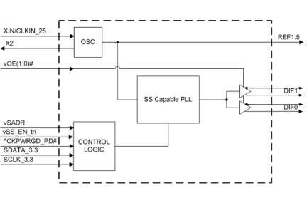
The 9FGU0231 is a member of IDT's 1.5 V Ultra-Low-Power PCIe clock family. The device has 2 output enables for clock management, 2 different spread spectrum levels in addition to spread off, and 2 selectable SMBus addresses.
特長
-
LP-HCSL outputs; save 4 resistors compared to standard PCIe devices
-
23 mW typical power consumption; reduced thermal concerns
-
OE# pins; support DIF power management
-
Programmable slew rate for each output; allows tuning for various line lengths
-
Programmable output amplitude; allows tuning for various application environments
-
DIF outputs blocked until PLL is locked; clean system start-up
-
Selectable 0%, -0.25% or -0.5% spread on DIF outputs; reduces EMI
-
External 25 MHz crystal; supports tight ppm with 0 ppm synthesis error
-
Configuration can be accomplished with strapping pins; SMBus interface not required for device control
-
3.3 V tolerant SMBus interface works with legacy controllers
-
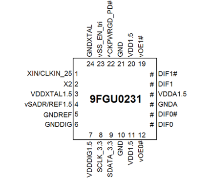
Space saving 4x4 mm 24-pin VFQFPN; minimal board space
-
Selectable SMBus addresses; multiple devices can easily share an SMBus segment
製品比較
アプリケーション
設計・開発
モデル
ECADモデル
[製品選択]テーブル内の製品名をクリックするとSamacSysが提供する回路図シンボル、PCBフットプリント、3D CADモデルがご確認いただけます。 お探しのシンボルやモデルが見つからない場合、Webサイトから直接リクエストできます。

製品選択
適用されたフィルター
ビデオ&トレーニング
PCIe Clocking Architectures (Common and Separate)
This is the first video in our PCIe series. In this video, we define PCIe architectures, focusing on common and separate clock architectures. Watch the rest of the video series below where Ron will cover the impact of different timing architectures.
Watch the Video Series Below
Video List


