概要
説明
The 9FGV1005 is a member of Renesas' PhiClock™ programmable clock generator family. The 9FGV1005 provides two copies of a single non-spread spectrum output frequency and one copy of the crystal reference input. Two select pins allow for hardware selection of the desired configuration, or two I²C bits all easy software selection of the desired configuration. The user may configure any one of the four OTP configurations as the default when operating in I²C mode. Four unique I²C addresses are available, allowing easy I²C access to multiple components.


特長
- PCIe Gen 1–5 compliant
- PCIe Gen 5 Common Clock jitter < 80fs RMS
- 284fs RMS typical phase jitter at 156.25MHz (12kHz to 20MHz)
- 2 programmable output pairs plus 1 LVCMOS REF outputs
- 1 integer output frequency per configuration
- 1MHz to 325MHz output frequency (LVDS or LP-HCSL)
- 1MHz to 200MHz output frequency (LVCMOS)
- 1.8V to 3.3V core VDD
- Individual 1.8V to 3.3V VDDO for each programmable output pair
- Supports HCSL, LVDS, and LVCMOS I/O standards
- Supports AC-coupled LVPECL and CML logic – See AN-891
- 3mm × 3mm 16-LGA packages with 50MHz integrated crystal option
- Supported by Timing Commander™ software
製品比較
アプリケーション
設計・開発
ソフトウェア/ツール
ボード&キット
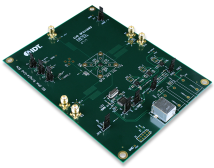
Evaluation Kit for 9FGV1005 Programmable PhiClock™ Generator with Internal 50MHz Crystal
This is the evaluation board for the 9FGV1005Q5 programmable PhiClockTM generator with internal 50MHz crystal. It provides a convenient way of configuring and...
モデル
ECADモデル
[製品選択]テーブル内の製品名をクリックするとSamacSysが提供する回路図シンボル、PCBフットプリント、3D CADモデルがご確認いただけます。 お探しのシンボルやモデルが見つからない場合、Webサイトから直接リクエストできます。

製品選択
適用されたフィルター
ビデオ&トレーニング
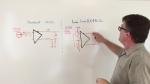
PCIe Reference Clock Jitter Budgets
Ron Wade, chief PCIe system architect explains the fundamental difference in reference clock jitter budgets between the first three generations of the specification and those of Gen4 and Gen5 which raise new challenges for designers.
Related Resources
Video List